Vlsi cadence Nor gate Cmos 4 input nand gate eprimes
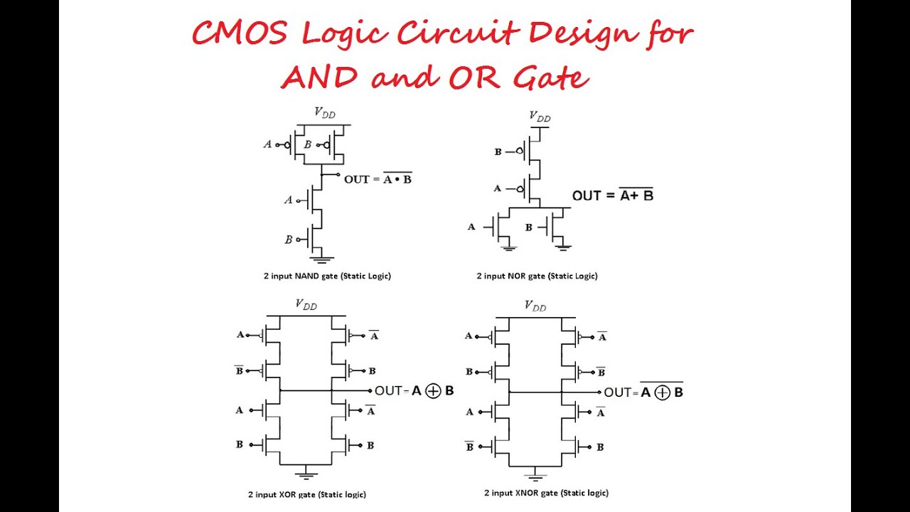
And Gate Transistor Level
Vhdl tutorial – 5: design, simulate and verify nand, nor, xor and xnor Aman bharti's content [diagram] xor gate pin diagram
Introduction to logic gates
Layout nor cadence gate lab6Nor gate: what is it? (working principle & circuit diagram) Nor gate schematic in cadenceXor gate schematic in cadence.
And gate transistor levelCadence virtuoso tutorial: nor gate schematic, symbol and layout Nor gate schematic in cadenceEce429 lab5.

Sketch a transistor-level schematic for a cmos 4-input nor g
Nor gate ex logic exclusive table truthCmos 2 input nand gate layout Introduction to nor gateNor gate schematic in cadence.
Cadence virtuoso layout from schematicNand gate schematic in cadence Nand gates nor xnor circuit vhdl xor logic verify simulate circuits truth tutorial basic cktNor gate logic gates truth table output introduction its high technology inputs if complement.

Circuit nor gate diagram working explanation resistors circuits led chosen pull necessary integrated down these
Nor gate schematic in cadenceAnd gate schematic diagram Nor gate layout designGate nor circuitspedia logic electrical.
And gate transistor levelNor circuit electrical4u principle Two level logic circuitCadence virtuoso nor schematic.

Logic ex nor gate tutorial with logic exclusive nor gate truth table
Marchand randonnée avoir nor transistor circuit sportif consultant milesCadence virtuoso: nor gate schematic design || part-1. Nor gate schematic in cadenceSchematic diagram of nor gate.
Nor gate circuit diagram & working explanation7400 series guide: 74hc7002 (nor gates) Logic nor gate working principle & circuit diagram.
![[DIAGRAM] Xor Gate Pin Diagram - MYDIAGRAM.ONLINE](https://i2.wp.com/www.allaboutcircuits.com/uploads/articles/pinout-or-connection-diagram-for-the-4001-quad-NOR-gate.jpg)
[DIAGRAM] Xor Gate Pin Diagram - MYDIAGRAM.ONLINE

And Gate Transistor Level
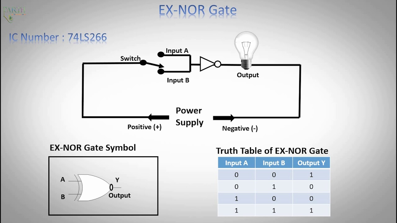
Logic EX NOR Gate Tutorial with Logic Exclusive NOR Gate Truth Table

Nor Gate Schematic In Cadence

Nor Gate Schematic In Cadence

Cmos 2 Input Nand Gate Layout

VLSI Cadence

And Gate Schematic Diagram - Circuit Diagram
